During my PhD, I spent countless hours in the clean room for fabricating my nanoelectronic devices. It’s rewarding to see your designs becoming a reality. I always found the microscopic “photographs” fascinating, and beautiful. Here, you can find a collection of my beloved devices with a short description of their purpose. For those non-technical readers, just appreciate the size of the features (see the scale bars; 1 μm = 1000x smaller than 1 mm).
After several design iterations, I finally found a working sample for performing key experiments for my PhD. For instance, I successfully observed antibunching, i.e. repulsion, between two individual flying electrons! This demonstration is huge for us because it lays the ground work for future implementations of in-flight manipulations. For more details, check out our Nature Nanotechnology paper!
Update: by adding more flying electrons, we observed signatures of an exotic liquid-like state! Check out our Nature publication!
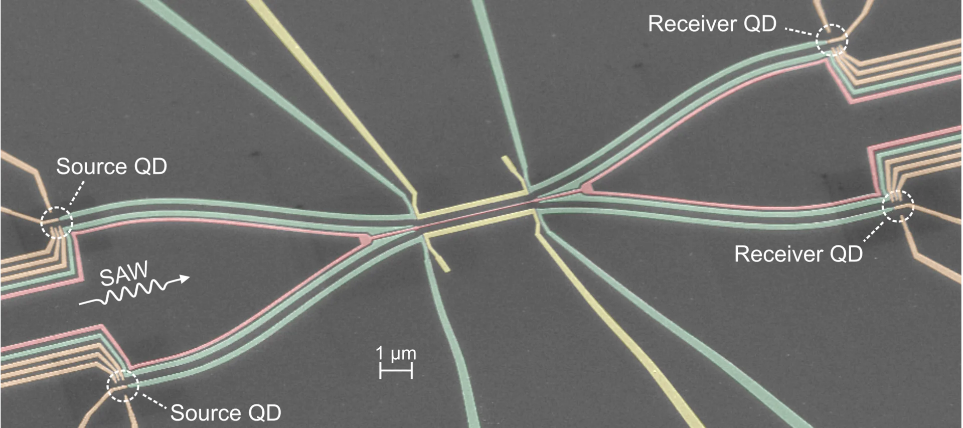
Personally, I love the spider-like shape of this device. I find it quite artistic! This design has two quantum dots (dashed circles) on both sides, acting as sources and receivers. The idea is to have an injection path as smooth as possible, while keeping full control of our single dot. As you can see, the metallic gates are densely packed and nanoscopic, which makes the nanofab quite challenging. Tests after tests, I finally ended up with a full basket of tricks which enhances its success rate. Let me emphasize that these tricks allowed me to have 100% yield for almost all my posterior fabs.
From the physics point of view, however, we realized that having a smooth injection actually is detrimental for our synchronization technique. To be specific, in order to send an electron with precise timing, we need to prepare it in a metastable position where it stays in the dot when the SAW passes. Then, to trigger the sending, we would send a very short voltage pulse to “kick it out”. So, here, the injection is so smooth that we could not actually have this “protected” position. This is why, in the next generation, HBT9, we abandoned the smooth injection idea.
This design was the first one to conceive the idea of smooth injection. This is actually an extension of the beautiful design employed for spin-transfer experiments using sound waves — see Jadot et al. Nat Nano (2021). Although the nanofab wasn’t perfect at this point (it was my first fully finished sample), the design had one main limitation: crosstalk between the electrometers (quantum dots at the left side of the green gates). Although I could have optimized the distances in the next generation, I decided that a double dot is not necessary for our experiments. Rather, it is better to have a full control of a single quantum dot.
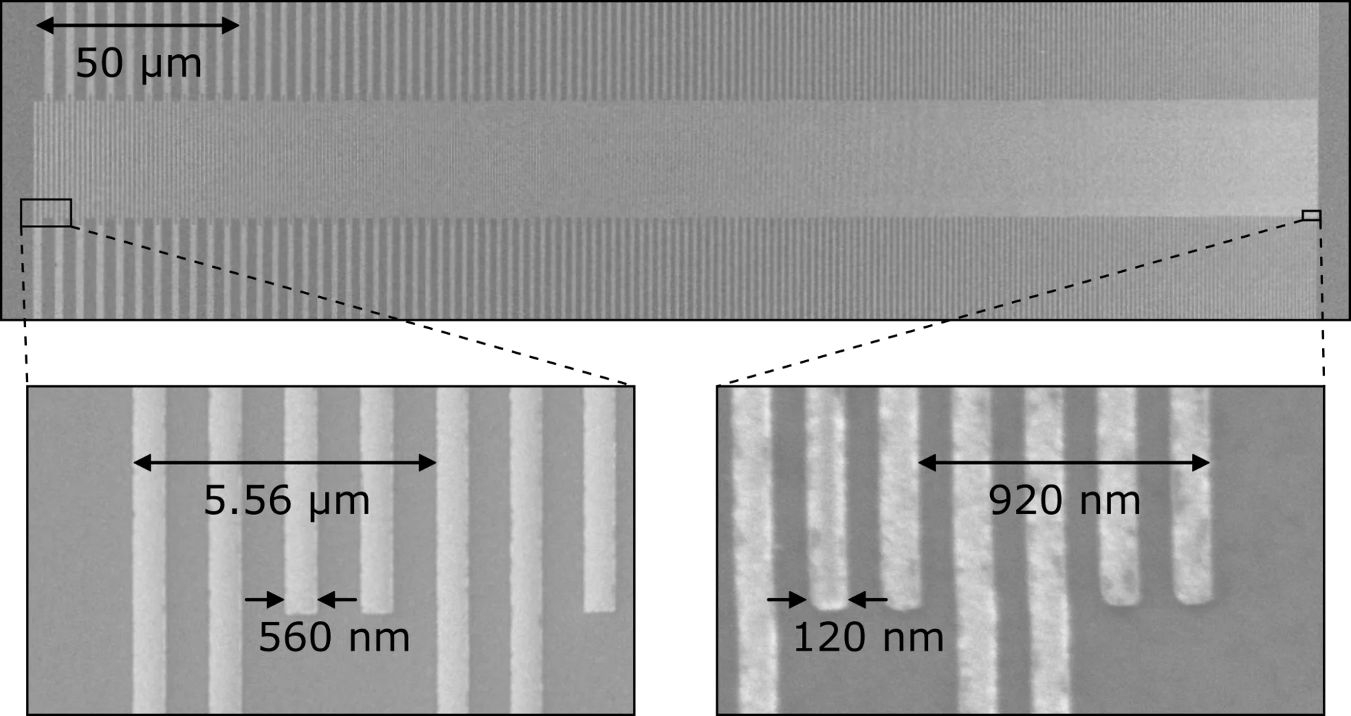
When I joined the group as an inexperienced internship student, the project I was assigned was: let’s compress the sound waves into a single pulse! Let me skip here the why of it, but focus on how. The device you see is called an interdigital transducer. The most important aspect is that the periodicity of the metallic fingers defines the frequency of the sound wave. In the most simple case, if the period is regular, then all the wave will superpose, resulting in a long sinusoidal acoustic wave. But, how can we can a single peak? Fourier told us that if you superpose many different frequencies in phase, basically you can have a delta Dirac function. To implement this idea, what we needed to do is to change gradually the period of the fingers, as you can see in the above images. As the chirping of a bird, this device is called chirp IDT.
From the nanofab perspective, the challenge is to have these hundreds of extremely narrow and densely packed electrodes no touching each others. Your main enemy during the electron lithography is the proximity effect, meaning that while you are “writing” the electrode pattern, some electrons also will spread at its surroundings. One of the key solutions is to reduce the each electrode pattern by actually 50% in the design.
After several optimizations, we finally demonstrated highly-efficient electron transfer with this acoustic pulse. Since sound waves are gaining popularity in many fields of physics, this technique can be easily implemented for other applications such as spintronics and photonic hybrid interfaces.
Check out the details in our PRX paper or the highlight in their non-technical article!
Furthermore, you can easily design your own IDTs using my Python package idtpy!
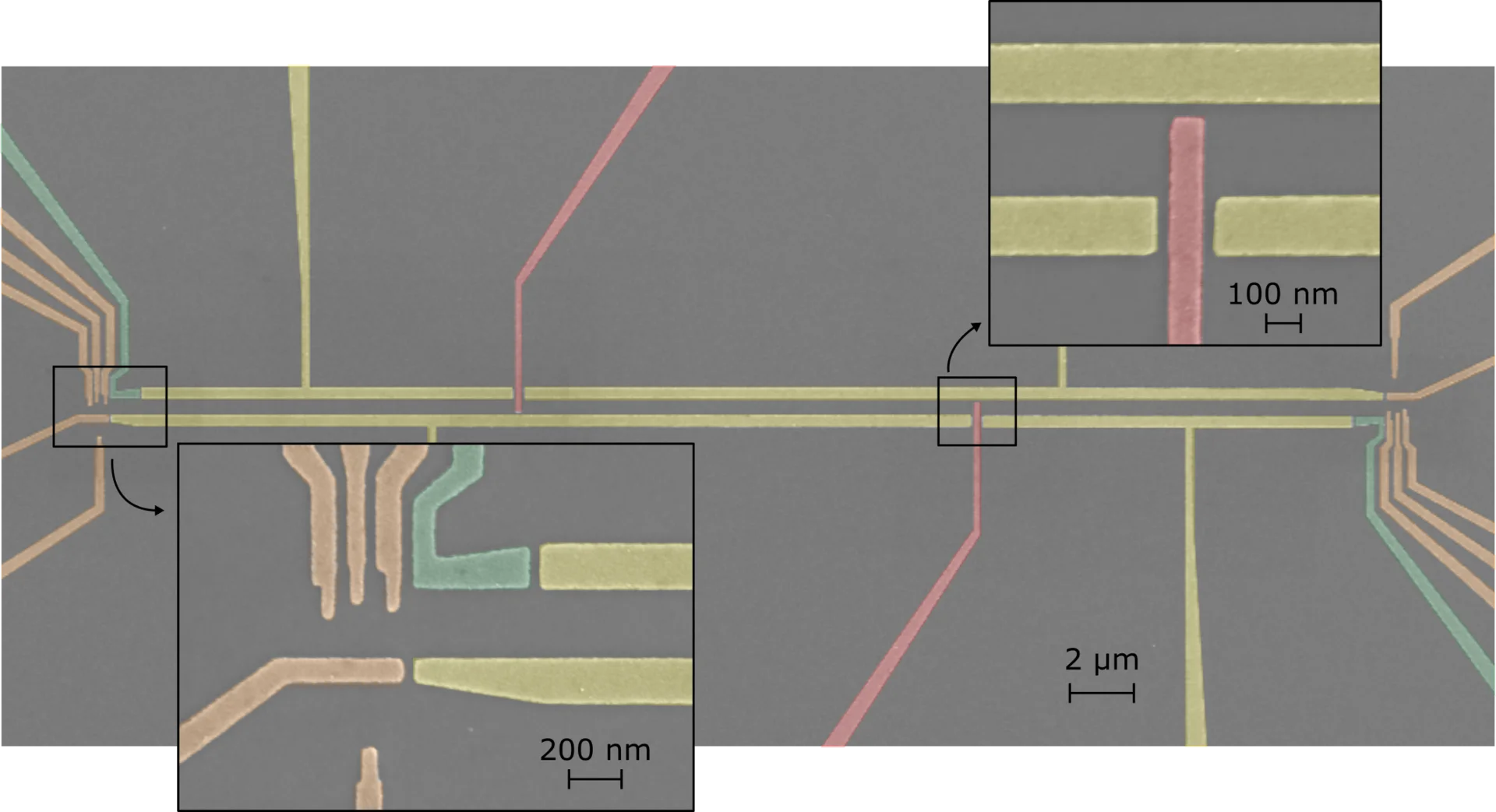
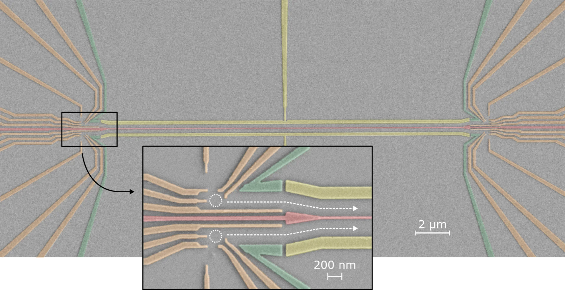
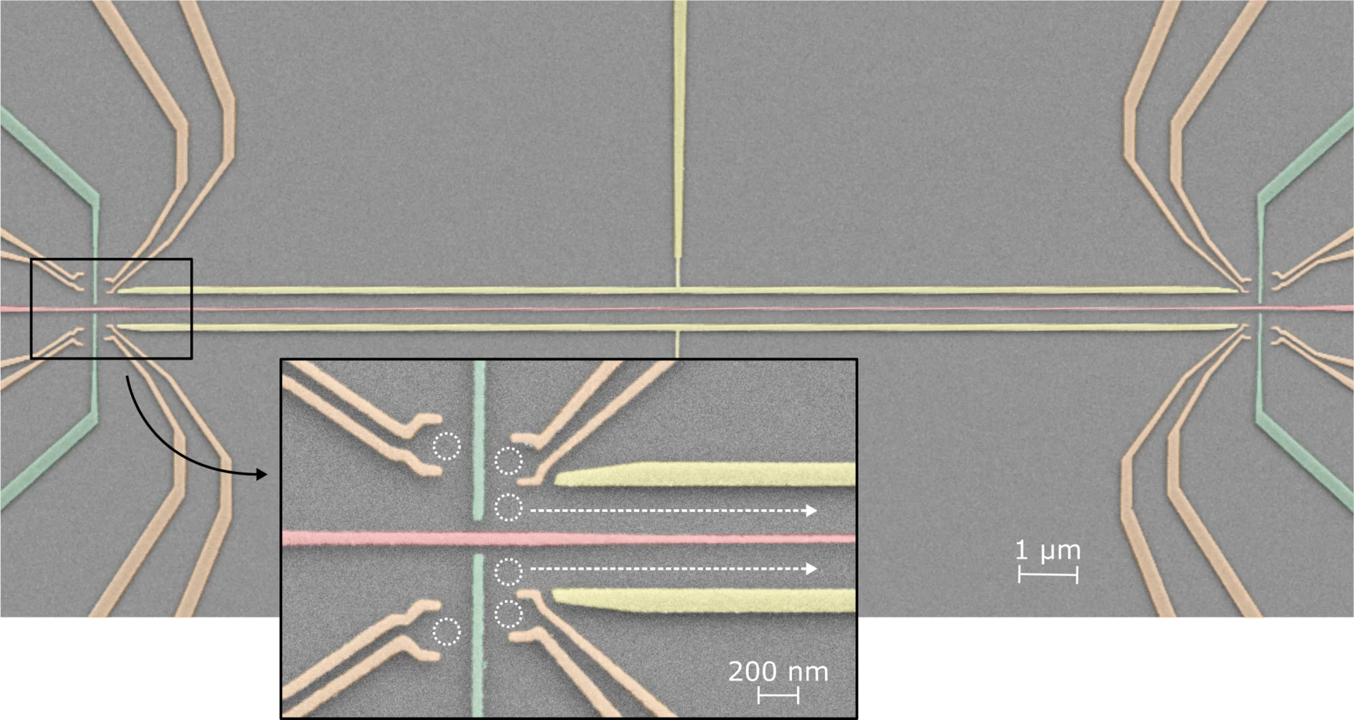
The way we know that the electron travels through our structure is by checking that one electron is lost at our source (left) and, correspondingly, we get an extra electron at our receiver (right). But, what happens in the middle? Does the electron get blocked? Or does it travel smoothly?
This sample answer those questions! The key element is the barriers (red gates) in the middle of the channel. The idea is to block/unblock the path with very fast voltage pulses (tens of picosecond). In other words, this is equivalent to take snapshots of the electron at those barrier locations! Combining two barriers allow us to further measure precisely the flight time of our electron!
For more technical details, check out our APL article!